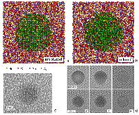
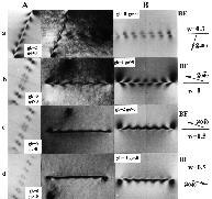
Ag-particle in glasses to
study migration, nucleation
and relaxation
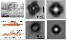
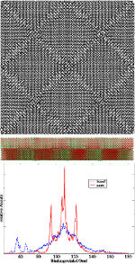
MD relaxed dots and HREM
image matching using
the simulated structures
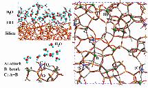
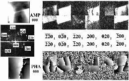
MD calculation of
silanoles created
by water on silica
surfaces
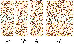
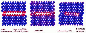
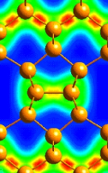
MD simulation of
Silica Waferbonding
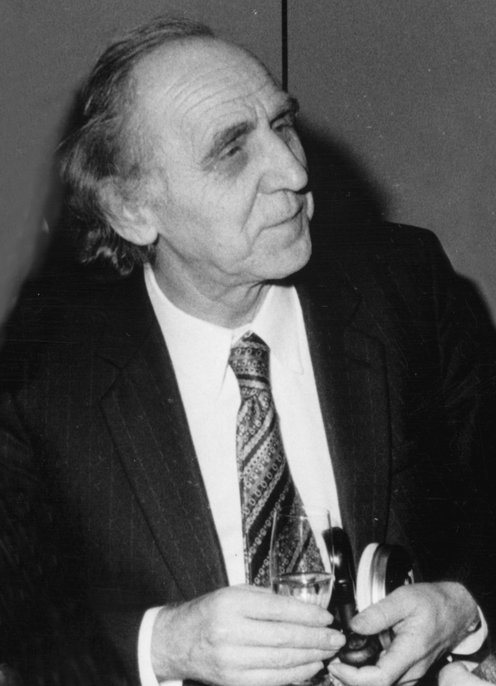
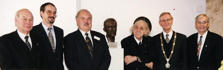
Working in the field of solid state physics I have made structure investigations applying Molecular Dynamics, Electron Microscopy and Electron Holography. The investigations I did during my employment from 1973 up to 2013 in the Institute of Solid State Physics and Electron Microscopy (AdW-IFE) in Halle (Saale), an Institute of the former Academy of Sciences of the GDR. The AdW-IFE was founded by Professor Heinz Bethge (cf. Bethge-Stiftung, Bethge-Mikroskop) and was in 1992 the basis of the Institute of Microstructure Physics (MPI-Halle) of the Max Planck Society of Germany (cf. especially former departements of the MPI-Halle, image of the founding directors).
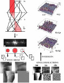
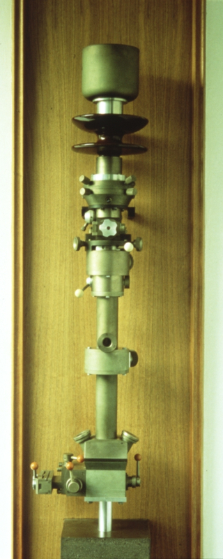
In short, I have investigated (cf. the figures below) the structure of interfaces, quantum dots, etc. in semiconductors and glasses as well as related problems as, e.g., the physical processes of wafer bonding by applying and combining High Resolution Electron Microscopy (HREM), Electron Holography and Molecular Dynamics (MD) simulations. HREM is a routine technique of the structural characterization of materials as it provides local information at an atomic level. Electron Holography allows enhanced structural studies to be carried out on the basis of the reconstructed aberration free complex wave function of the object. MD simulations enable theoretical investigations to be made of atomic interactions, including structural relaxations and dynamic processes, and thus the simulation of resulting physical properties. It was the main aim to theoretically improve the atomistic structure description to enable the extension of systems to macroscopically relevant ones as well as the development of semiempirical potentials which include the quantum effects of bonding and are relevant for inhomogeneities, surfaces and interfaces. In addition, I applied simulation and alternative reconstruction techniques and I have tried to develope an inverse object retrieval for the electron microscopic structure investigation to overcome the trial-and-error image matching.
The details can be found in my published paper, cf. papers&books and poster&talks.
Also some of my results may be found at the webpages of the former departements
of the MPI-Halle, especially former departement2 and the dept2-publications,
as well as due to the details of some of my former webpages, still existing at MPI-Halle:
- MD oft Wafer bonded Interfaces,
- Bond Order Potential and Inverse TEM-Problem,
- MD of Glasses & Small Particles, and
- MD of Quantum Wells & Dots